Platform Technology for High Speed Coating –
Any solid, on any substrate
PLASMAfusion® is a first of its kind, patented manufacturing platform technology developed by Oxford, UK based Plasma App Ltd, a wholly owned subsidiary of Meta Materials Inc. PLASMAfusion® enables high speed coating of any solid material on any substrate. It uniquely enables doping, multilayering, or mixing of materials in vacuum with controlled stoichiometry distribution within the deposited film at low substrate temperature.
Benefits:
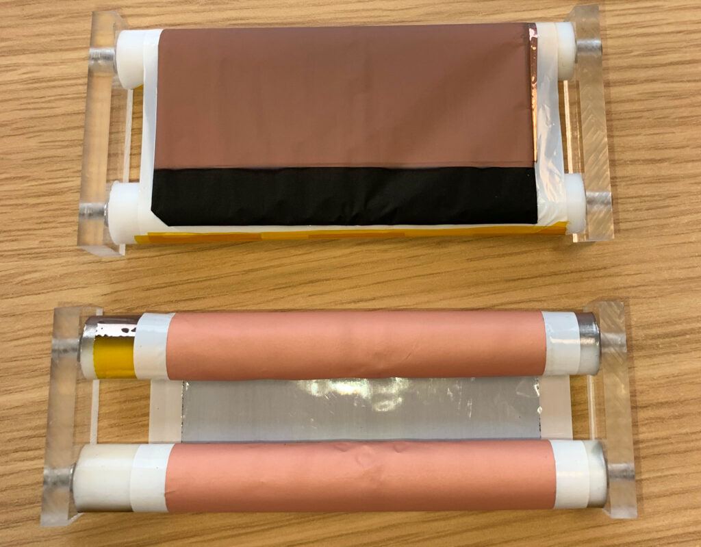
META expects to apply PLASMAfusion® to the metallization step in its roll-to-roll production process for NANOWEB® films as well as KolourOptik® security films. This is expected to significantly accelerate line speed and increase annual capacity. Large scale and efficient metallization is a critical step for volume production of NANOWEB® and many other high volume potential applications such as lithium-ion battery components. Large scale metallization is expected to leverage capital equipment investment and substantially reduce cost per square meter of output. META intends to continue to industrialize and scale up PLASMAfusion® including applications for its high volume factory in Thurso, Quebec. Additionally, PLASMAfusion® will be available for licensing and co-development for strategic partners.
Sustainable, Breakthrough Performance
PLASMAfusion® creates unprecedented new high-performance nanocomposites in real time by using multiple, time sequenced targets. This is a unique process enabler, likely to facilitate META’s entry into multiple high-growth markets. High energy beam deposition of materials, at low temperature, without solvents and other toxic chemicals, promises highly sustainable, breakthrough performance. Compared to traditional coating technologies, we estimate PLASMAfusion® is approximately 60x more energy efficient compared to Plasma Laser Deposition (PLD) and 8x more efficient compared to Magnetron Sputtering to produce each 100nm of coating on each square cm area of the substrate, while also offering higher adhesion, deposition rates, and overall coating uniformity.
Platform Technology

- Thin or thick films
- Any material
- Low substrate temperature
- High deposition rate
- Superior adhesion
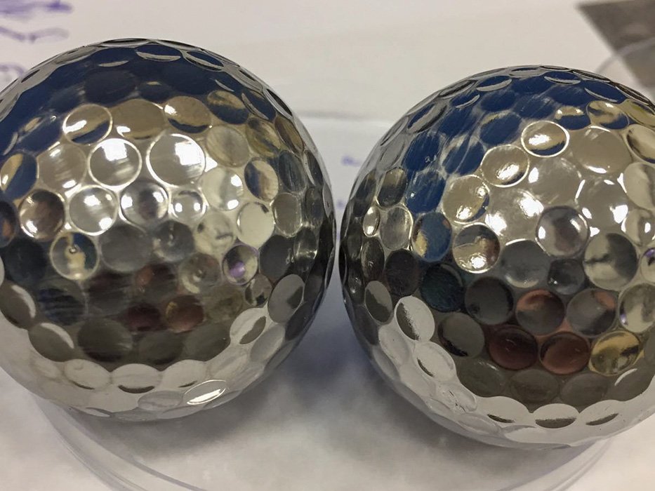
PLASMAfusion® 10 Second Demonstration
- Deposition of Stainless Steel
- On a golf ball
- 10 seconds – 100 nanometers
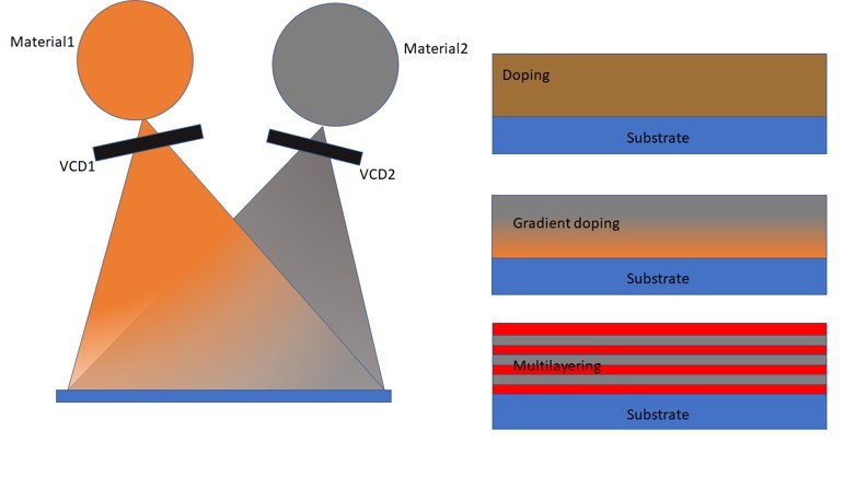
Two-Source PLASMAfusion®
Computer controlled two-source operation enables independent control of each source. Operating parameters enable the design of the deposited films for doping, gradient doping, and multilayered structures.
Applications
PLASMAfusion® enables design of surfaces and a path to industrial surface manufacturing for a variety of applications.
Batteries
- Electrode manufacturing
- Composite anode/cathode
- Solid state battery
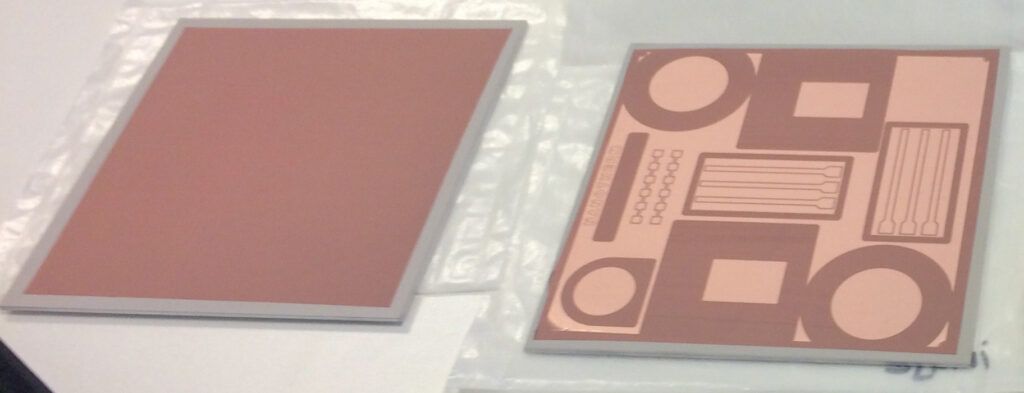
Printed Circuit Boards
- Thick metal layer deposition on ceramics
- Low temperature substrates
- Interfaces with gradient materials mixing
- Metallized PTFE for high frequency apps
Semiconductors & Metamaterials
- Thin/thick films with improved interfaces
- Semiconductor gradient doping
- Complex multi-layer designs
- Extreme parameter metamaterials (anisotropic, hyperbolic, topological, etc.)
Protective/Optical Coatings
- Multi-layer barriers at low cost
- Complex stoichiometry materials
- Oxides, polymer, and hard coatings
- Anti-reflective and hydrophobic coatings
Examples
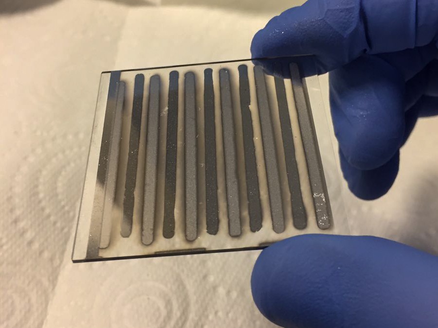
Pictured below are some examples of PLASMAfusion® applications, including stainless steel on plastic, copper on ceramic substrates, a prototype Li ion battery anode, and a thermoelectric generator prototype.
Prototype Li Ion Battery Anode
Plasma App has been developing next generation battery materials for several years with partners. The prototype Li ion battery anode pictured here was fabricated by PLASMAfusion® of CALIB anode active material on a 25 µ standard battery separator followed by deposition of a 2 µ copper current collector.
Results were published in January 2021 in Nano Energy 83 (2021) 105816. The technology is described in this publication as virtual cathode deposition. This work was supported by Innovate UK Project number 133374.
Thermoelectric Generator Prototype
A proof-of-concept Bi2Te3 and Bi0.5Sb1.5Te3 TEG (thermoelectric generator) prototype was fabricated using dual source PLASMAfusion®.
- S per pair of 250 μV/K
- Power ~1 nW for 4.5 pairs @20° C
Results were published in March 2019 in Scientific Reports (2019) 9:4393. The technology is described in this publication as virtual cathode deposition.
PLASMAfusion® Technique
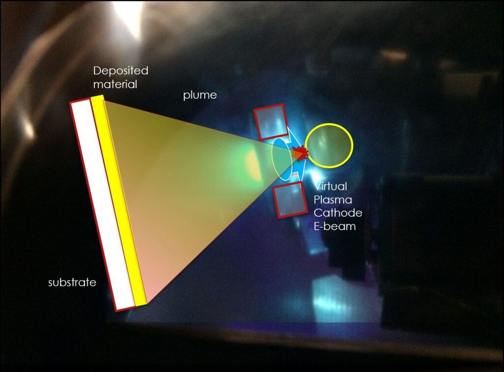
PLASMAfusion® uses a pulsed electron beam in a mid-range vacuum to ablate a solid-state target containing the source material(s). Unlike the typical channel-spark discharge deposition, which is limited by the short lifetime of the cathode, PLASMAfusion® deploys a virtual plasma cathode which is generated prior to each pulse of the electron beam. Each PLASMAfusion® pulse begins with a generation of plasma through ionization of the operation gas. The electron beam ablates the target and then the plasma cathode decays, leaving a space for ablated target material in the form of a plasma plume to propagate toward a substrate, where it forms a film. Repetition of the pulse at a rate in the range of 1–600 Hz allows a film to grow on the substrate with controlled growth rate and properties.